- 您现在的位置:买卖IC网 > Sheet目录1223 > KIT10XS3535EVBE (Freescale Semiconductor)KIT EVAL BOARD FOR 10XS3535
�� �
�
�FUNCTIONAL� DEVICE� OPERATION�
�LOGIC� COMMANDS� AND� REGISTERS�
�LOGIC� COMMANDS� AND� REGISTERS�
�SERIAL� INPUT� COMMUNICATION�
�SPI� communication� compliant� to� 3.3� V� and� 5.0� V� is�
�?�
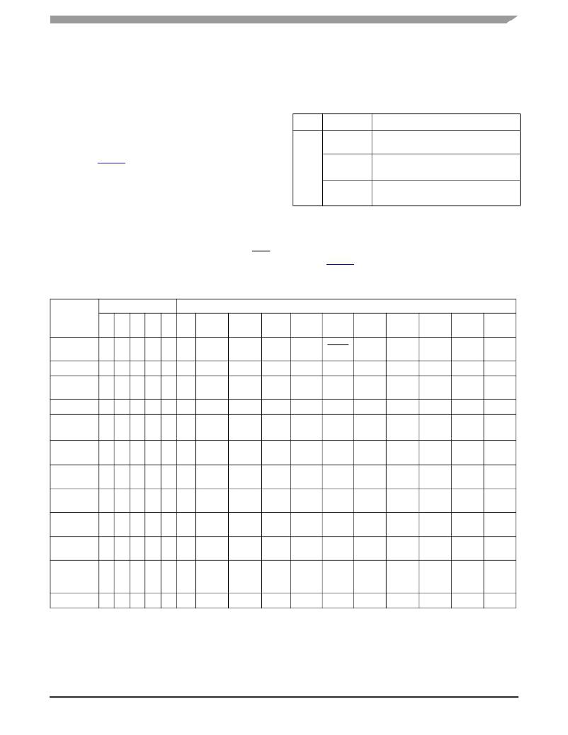
�Table� 7.� SI� Message� Bit� Assignment�
�accomplished� using� 16-bit� messages.� A� message� is�
�transmitted� by� the� master� starting� with� the� MSB,� D15,� and�
�ending� with� the� LSB,� D0.� Each� incoming� command� message�
�Bit� Sig�
�MSB�
�SI� Msg� Bit�
�D15� :� D11�
�Message� Bit� Description�
�Register� address� bits.�
�on� the� SI� pin� can� be� interpreted� using� the� bit� assignment�
�described� in� Table 7� .� The� 5� bits� D15� :� D11,� called� register�
�address� bits,� are� used� to� select� the� command� register.� Bit�
�D10�
�Watchdog� in:� toggled� to� satisfy� watchdog�
�requirements.�
�D10� is� the� watchdog� bit.� The� remaining� 10� bits,� D9� :� D0,� are�
�used� to� configure� and� control� the� output� and� its� protection�
�features.� Multiple� messages� can� be� transmitted� in�
�LSB�
�D9� :� D0�
�Used� to� configure� inputs,� outputs,� device�
�protection� features,� and� SO� status� content.�
�succession� to� accommodate� those� applications� where� daisy�
�chaining� is� desirable� or� to� confirm� transmitted� data� as� long� as�
�the� messages� are� all� multiples� of� 16� bits.� Any� attempt� made�
�to� latch� in� a� message� that� is� not� 16� bits� will� be� ignored.�
�All� SPI� registers� are� reset� (all� bit� equal� 0)� in� case� of� RST�
�equal� 0� or� fail� mode� (Fail=1).�
�DEVICE� REGISTER� ADDRESSING�
�The� register� addresses� (D15� :� D11)� and� the� impact� of� the�
�serial� input� registers� on� device� operation� are� described� in� this�
�section.� Table 8� summarizes� the� SI� registers.�
�Table� 8.� Serial� Input� Address� and� Configuration� Bit� Map�
�SI� Address�
�SI� Data�
�SI� Register�
�D1� D1� D1� D1� D1�
�5� 4� 3� 2� 1�
�D10�
�D9�
�D8�
�D7�
�D6�
�D5�
�D4�
�D3�
�D2�
�D1�
�D0�
�Initialization�
�0�
�0�
�0�
�0�
�0�
�WD�
�0�
�0�
�FOGen�
�PWM�
�sync�
�Xenon�
�MUX2�
�MUX1�
�MUX0�
�SOA1�
�SOA0�
�Config� OL�
�0�
�0�
�0�
�0�
�1�
�WD�
�LEDControl5�
�0�
�0�
�0�
�LEDControl1�
�OLLED5� OLLED4� OLLED3� OLLED2� OLLED1�
�Config�
�Prescaler�
�Config� SR�
�0�
�0�
�0�
�0�
�0�
�0�
�1�
�1�
�0�
�0�
�WD�
�WD�
�0�
�1�
�PR1�
�SR1�
�PR2�
�SR2�
�PR3�
�SR3�
�0�
�0�
�0�
�0�
�0�
�0�
�PR4�
�SR4�
�PR5�
�SR5�
�PR6�
�0�
�Config� CSNS� 0�
�0�
�0�
�1�
�1�
�WD�
�CSNS�
�sync�
�0�
�0�
�0�
�0�
�NO_OCHI5� NO_OCHI4� NO_OCHI3� NO_OCHI2� NO_OCHI1�
�Control�
�OUT1�
�Control�
�OUT2�
�Control�
�OUT3�
�Control�
�OUT4�
�Control�
�OUT5�
�0�
�0�
�0�
�0�
�0�
�1�
�1�
�1�
�1�
�1�
�0�
�0�
�0�
�1�
�1�
�0�
�1�
�1�
�0�
�0�
�1�
�0�
�1�
�0�
�1�
�WD� Phase2�
�WD� Phase2�
�WD� Phase2�
�WD� Phase2�
�WD� Phase2�
�Phase1�
�Phase1�
�Phase1�
�Phase1�
�Phase1�
�ONoff�
�ONoff�
�ONoff�
�ONoff�
�ONoff�
�PWM6�
�PWM6�
�PWM6�
�PWM6�
�PWM6�
�PWM5�
�PWM5�
�PWM5�
�PWM5�
�PWM5�
�PWM4�
�PWM4�
�PWM4�
�PWM4�
�PWM4�
�PWM3�
�PWM3�
�PWM3�
�PWM3�
�PWM3�
�PWM2�
�PWM2�
�PWM2�
�PWM2�
�PWM2�
�PWM1�
�PWM1�
�PWM1�
�PWM1�
�PWM1�
�PWM0�
�PWM0�
�PWM0�
�PWM0�
�PWM0�
�Control�
�External�
�0�
�1�
�1�
�1�
�0�
�WD� Phase2�
�Phase1�
�ONoff�
�PWM6�
�PWM5�
�PWM4�
�PWM3�
�PWM2�
�PWM1�
�PWM0�
�Switch�
�RESET�
�X�
�X�
�X�
�X�
�X�
�0�
�0�
�0�
�0�
�0�
�0�
�0�
�0�
�0�
�0�
�0�
�Note:� testmode� address� used� only� by� FSL� is� D[15:11]=01111� with� RST� pin� voltage� higher� than� 8V� typ.�
�X� =� Don’t� care� and� 0� =� need� to� rewrite� logic� “0”�
�MC10XS3535�
�Analog� Integrated� Circuit� Device� Data� ?�
�Freescale� Semiconductor�
�29�
�发布紧急采购,3分钟左右您将得到回复。
相关PDF资料
KIT13892VLEVBEJ
KIT EVAL FOR MC13892
KIT17C724EPEVBE
KIT FOR 17C7242CH HBRIDGE PWR IC
KIT33810EKEVME
BOARD EVAL FOR MC33810
KIT33811EGEVBE
KIT EVAL 33811 SOLENOID MON IC
KIT33812ECUEVME
KIT DESIGN FOR 33812/S12P
KIT33812EKEVBE
BOARD EVALUATION FOR MC33812
KIT33879AEKEVBE
BOARD EVALUATION FOR MC33879
KIT33880DWBEVB
KIT EVAL FOR MC33880 8X SW W/SPI
相关代理商/技术参数
KIT10XS4200EVBE
制造商:Freescale Semiconductor 功能描述:EVAL BOARD, MC10XS4200 HIGH SIDE SWITCH; Silicon Manufacturer:Freescale; Silicon Core Number:MC10XS4200; Kit Application Type:High Side Switch; Application Sub Type:-; Kit Contents:Eval Board MC10XS4200, CD ROM
KIT-1113C
制造商:ABIKO 功能描述:Bulk
KIT1116-400
制造商:Laird Technologies Inc 功能描述:ANTKIT,FG 128-137MHZ/ODB + FM2
KIT-113-175C
制造商:LG Corporation 功能描述:KIT TUNER 113-175C (113-175E +
KIT1133-P250
功能描述:ANTKIT GB8W15FT CABLE 制造商:laird technologies ias 系列:* 零件状态:在售 标准包装:1
KIT-11591
功能描述:ISP POGO ADAPTER KIT 制造商:sparkfun electronics 系列:- 零件状态:在售 套件类型:初级入门套件 主要用途:ISP Pogo 适配器 标准包装:1
KIT1167-120
制造商:Laird Technologies Inc 功能描述:ANT KIT GPS1575PW 20FT 制造商:Laird Technologies Inc 功能描述:ANTKIT,GPS1575PW/20FT
KIT1185-120
制造商:Laird Technologies Inc 功能描述:KIT ANT GPS 20FT 制造商:Laird Technologies Inc 功能描述:KIT1185-120